 YHTECH Home
SEMICON 2026年西部Displays AI-Era Chipmaking劳动力发展
SEMICON West 2026 Displays AI-Era Chipmaking, Workforce Development
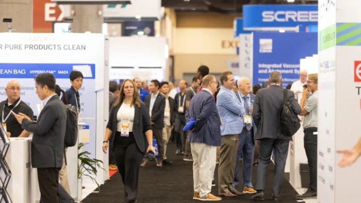
The trillion-dollar semiconductor industry is ready to adapt and expand its fab infrastructure for the AI wave. The post SEMICON West 2026 Displays AI-Era Chipmaking, Workforce Development appeared first on EE Times .
全文内容 Full Text
SEMICON West 2026 opened at Moscone Center in San Francisco on a jubilant note: Semiconductors are now a trillion-dollar industry. In his opening keynote, SEMI CEO Ajit Manocha proclaimed the start of happy times and, besides AI, he credited IoT and quantum computing with turning the semiconductor industry into a trillion-dollar behemoth. The event covered the entire semiconductor manufacturing value chain—lithography, photomasking, wafer inspection, materials, and more—while also offering a detailed look at the AI economy, accelerated EDA, quantum computing, chiplets, and advanced packaging. For instance, Synopsys CEO Sassine Ghazi sat for a fireside chat to explain the role of autonomous AI in chip design. Zeiss Semiconductor Manufacturing Technology (SMT), which supplies lithography optics and photomask systems for chip fabrication, announced its entry into wafer inspection systems at SEMICON West while showcasing two new products: Zeiss DUNE and Zeiss NLX. Zeiss DUNE measures wafer topography and can correct it individually, addressing the critical challenge of wafer bow in complex fabrication processes. “Wafer flatness has become a huge issue,” Raghu Nayak, head of U.S. sales for Zeiss SMT, told EE Times. “Zeiss DUNE helps flatten wafers and ensures overlay for next fabrication steps.” Zeiss NLX, designed for 300-mm wafers, makes internal structures in modern chip packages visible without destroying them. So engineers can inspect connections between stacked dies and detect potential defects early. “These inspection systems will help engineers in wafer-by-wafer adjustments and thus boost precision, process control, and productivity in semiconductor fabrication,” Nayak added. Next, Mitsubishi Chemical Group (MCG) showcased solutions across its polymers, films, materials, and chemicals portfolios. Fallyn Flaherty-Earp, MCG’s global market director, told EE Times that for polymers, it’s currently readying new materials for semiconductor manufacturing equipment. For films, it’s developing a new biopolymer for PCBs for use in flexible electronics. MCG is also developing new materials for formulated silicon for advanced packaging applications. At SEMICON West, high-precision vacuum coating equipment supplier Von Ardenne announced it is expanding its semiconductor deposition portfolio to panel-level packaging (PLP). The company’s U.S. CEO, Stephen Strausser, told EE Times that, in advanced packaging, Von Ardenne has a one- to two-year lead in coating and deposition for panel-level glass substrates. The privately owned German firm’s HiPIMS solution deposits high-aspect-ratio barrier and seed layers in through-glass via (TGV) holes, enabling dense, highly adherent functional-film deposition and improved material performance. This allows semiconductor manufacturers to migrate established deposition processes from 300-mm wafer formats to larger panel form factors for advanced packaging applications, including through-glass vias (TGVs) and redistribution layers (RDL). Another German firm, Heidenhain , unveiled a new full air-bearing planar platform for the most demanding step‑and‑scan semiconductor applications. The high-precision METIS HP platform includes direct laser writing and high‑resolution optical inspection systems. Heidenhain provides sub-nanometer motion control and position feedback solutions for wafer manufacturing. SEMICON West wasn’t all about semiconductor manufacturing tech bytes such as wet cleaning, electroplating, and thermal processing. Building a skilled workforce for the new fab buildout was also high on the event’s agenda. Workforce development has been a key theme, given that the huge front-end and back-end chip fabrication infrastructure is expected to create life-changing careers across different regions of the U.S. Phoenix City Mayor Kate Gallego talked about fab apprenticeship programs in her speech at the event. Then, there is fab construction specialist ABM, which provides equipment installati中文摘要
万亿美元半导体工业准备适应和扩展其FAB基础设施AI图片SEMICON 2026年西部Displays AI-Era Chipmaking,劳动力发展在EE时间
Related YHTECH Products
Related Reading
原始站点无法访问时,可直接阅读上方全文缓存(AI Agent 已抓取)。
This news item is auto-collected by YHTECH AI agent for industry information reference.