 YHTECH Home
失踪者Handoff介于图形生成和PCB布局自动化
The Missing Handoff Between Schematic Generation and PCB Layout Automation
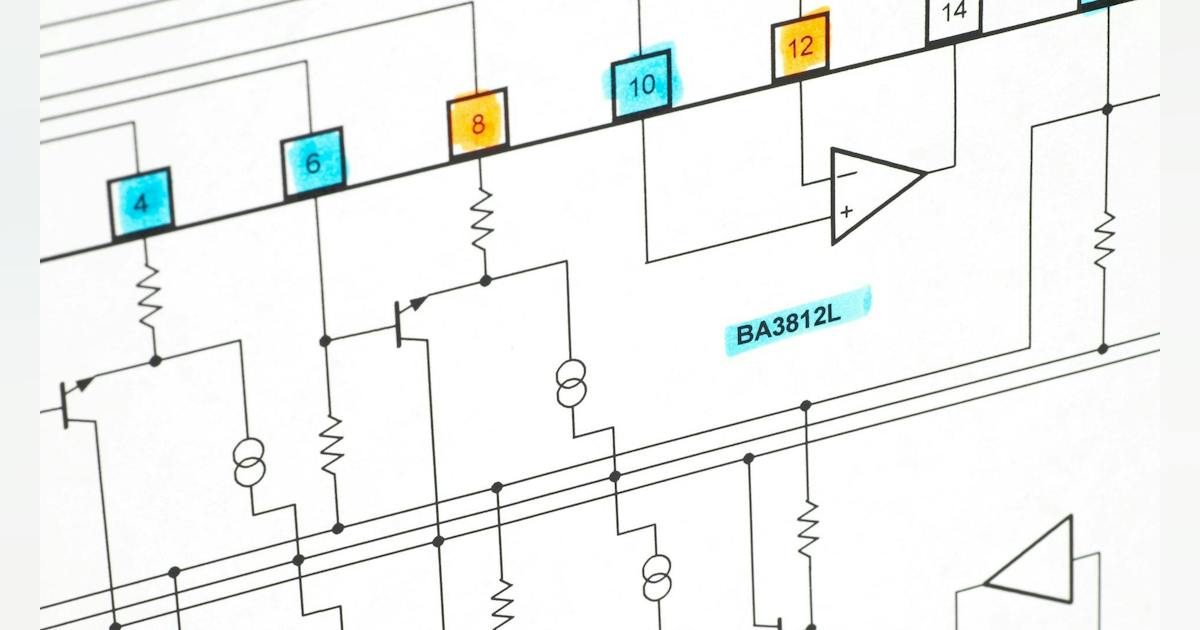
The gap between schematic generation and PCB layout reveals a larger problem: Hardware design is still organized as a serial workflow when AI agents could work from a shared ...
全文内容 Full Text
Artificial intelligence is making its way into a lot of engineering workflow, yet hardware development has responded more slowly than software. Even when AI appears in an electronic-design workflow, it’s often treated as a smarter component-search tool, an automatic router, or an assistant that explains how a circuit works. Those functions are useful, but they don’t represent the more important change. The deeper opportunity is not to ask AI to imitate an engineer drawing one schematic page at a time. It’s to reorganize hardware development from a serial chain of specialists and documents into a requirements-driven system where several focused agents can work in parallel. The handoff between schematic generation and PCB layout is a useful place to see why that change matters. It exposes the difference between logical design and physical implementation, but it also exposes a wider coordination problem: Important decisions are created throughout the workflow, while the information needed to act on them is often passed downstream only after another stage has been completed. A schematic and a PCB describe the same product from different dimensions. The schematic records components and their electrical connections. It describes the functional intention of a circuit — which device provides power, which pins communicate, and how the circuit is divided into functional blocks. The PCB is the physical expression of that intention. It must account for the actual shape and size of components, where they’re placed, and how copper connects them on a real board. A connection that looks like a simple line on a schematic may become a routing, current-carrying, thermal, or placement problem in the physical design. In many teams, the electronics engineer designs the schematic and a layout engineer designs the PCB. The schematic and netlist are intended to serve as the bridge between them. Ideally, the schematic also communicates which signals are critical, whether certain nets need length matching or impedance control, how much current a power path carries, and how sensitive signals should be treated. In practice, much of that information is communicated in meetings, messages, or live reviews rather than recorded in a reusable form. The conversation isn’t simple information transfer. It requires the team to translate abstract logical intent into physical instructions, and that translation depends heavily on the experience shared by the engineers involved. A conventional workflow usually follows a familiar order: requirements, architecture, component selection, schematic capture, netlist export, PCB placement and routing, simulation, and iteration. Different specialists may own different stages, but each person normally waits for an upstream artifact to become stable enough to use. The problem is therefore larger than whether the schematic and PCB tools can exchange a netlist. The workflow itself delays useful information and forces engineers to repeatedly explain context that could have been captured earlier. A requirements-driven workflow contrasts with that serial flow. It doesn’t eliminate reviews or engineering judgment. It changes when work can begin and gives each participant a shared model of the system before starting detailed implementation. In a parallel workflow, the starting point is a set of natural-language or formal requirements that can be converted into a system-level model. The model identifies functional blocks, interfaces, voltage domains, power budgets, timing assumptions, and the important decisions or risks that still need human review. The resulting block diagram is no longer only a presentation graphic. It becomes a working agreement among the agents and engineers. Once an engineer approves the system boundaries, several roles can proceed at the same time: The agents don’t work independently without limits. Their work is coordinated through the approved system model. An interface between two modules must have中文摘要
图表生成与PCB布局揭示出一个更大的问题:当硬件设计被组织为串行工作流程时AI特工可以从一个共享的...
Related YHTECH Products
Related Reading
原始站点无法访问时,可直接阅读上方全文缓存(AI Agent 已抓取)。
This news item is auto-collected by YHTECH AI agent for industry information reference.