 YHTECH Home
ZEISS SMT从Lithography Optics进入高级包装流程控制
ZEISS SMT Expands from Lithography Optics into Advanced Packaging Process Control
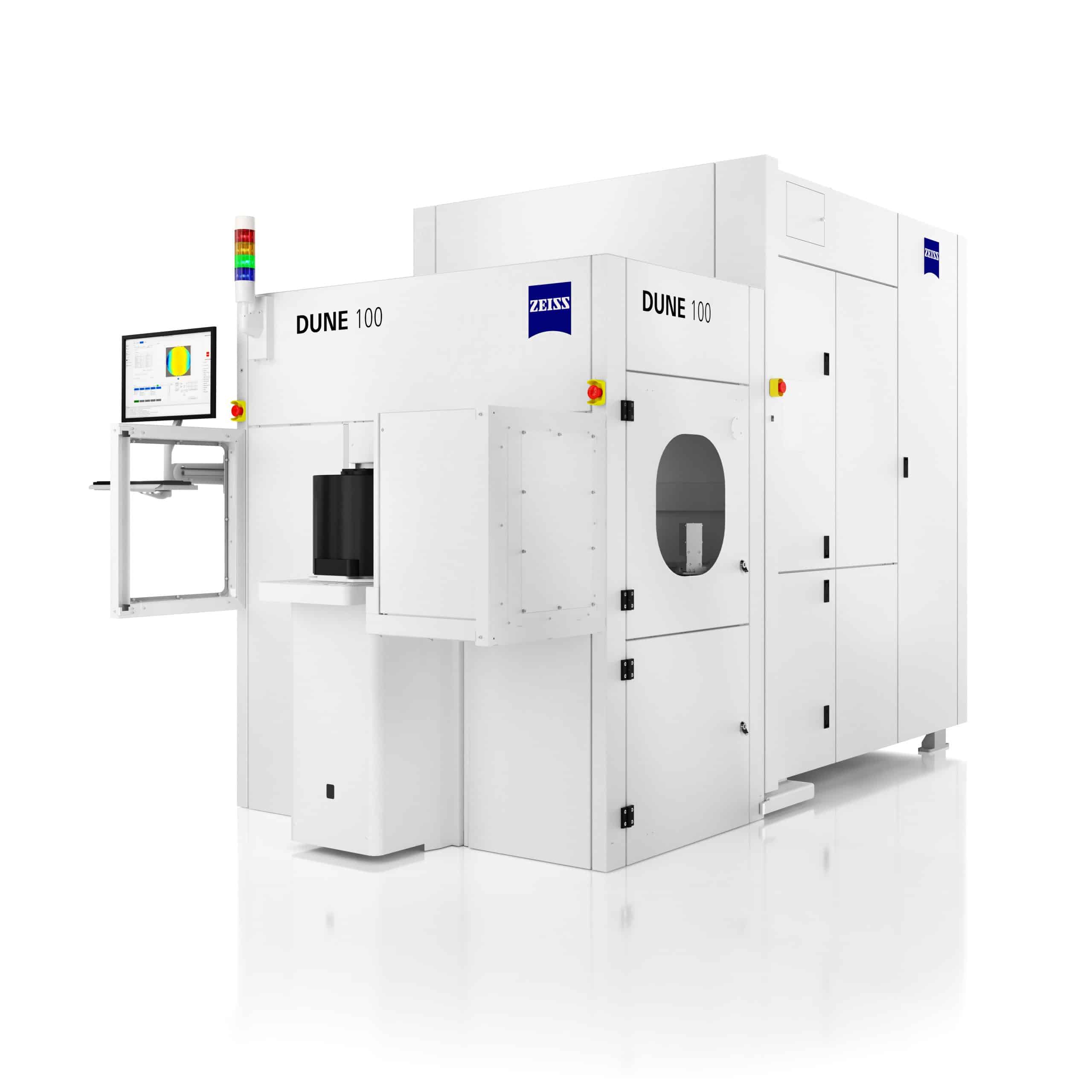
DUNE corrects wafer bow one wafer at a time, NLX brings X-ray inline, and mask tools get ready for High-NA's larger reticles The post ZEISS SMT Expands from Lithography Optics into Advanced Packaging Process Control appeared first on Semiconductor Digest .
全文内容 Full Text
Home » ZEISS SMT Expands from Lithography Optics into Advanced Packaging Process Control ZEISS is best known in semiconductors for the optics inside ASML’s lithography scanners, but ZEISS Semiconductor Manufacturing Technology (SMT) has been steadily building out a broader portfolio. “We have been the longest in supplying optics to ASML,” said Raghu Nayak, head of sales, North America. The company also supplies inspection optics, and for about a decade it has sold photomask tools. Its newest business, Semiconductor Fab Solutions, covers wafer inspection and metrology for both the front end and advanced packaging. ZEISS DUNE tackles wafer bow, which is critical when stacking wafers and dies. “Your wafers need to be as flat as possible. Ideally, 0% bow or cylinder or saddle,” Nayak said. Competing approaches apply backside coatings in a batch process for a global correction. DUNE measures each wafer and corrects it individually in the same process flow ( FIGURE 1 ). It works by focusing a laser at a controlled depth below the wafer’s backside surface. The interaction creates a localized plasma in the silicon, which is controlled to bring the wafer back to flat. Because it works from the back, the front side is untouched. Nayak said demos across logic and memory have shown no impact on the device side. The approach borrows from ZEISS’s mask business, where lasers have been used to correct photomask imperfections for more than 10 years. “All the leading foundries, memory makers and IDMs are looking into it actively,” he said. ZEISS NLX brings X-ray inspection from the failure analysis lab, where Nayak said ZEISS is the gold standard for nondestructive package analysis, to the production line. ZEISS isn’t the only company offering inline X-ray, but Nayak said it is unusual in owning the entire stack: source, platform, optics, hardware modules and software. The first systems have been built, with one at ZEISS’s Korea innovation center and another in active use in North America. Initial use cases include voids in through-silicon vias and in bonds, which become more critical as hybrid bonding shrinks void tolerances. Customers are also asking about X-ray for overlay. “As we move down to hybrid bonding and smaller structures, infrared, which is the technology right now used for overlay, is running out of steam,” he said. ZEISS also offers Intuitive 3D, a 300 mm FIB-SEM platform for 3D analysis that mills and images at the same time rather than alternating. The tool is destructive, but it can collect data on hundreds of 3D NAND cells rather than one. “So you have statistics now, and then you can figure out what your process window and process control need to look like,” Nayak said. On the mask side, ZEISS’s flow includes PROVE for registration metrology, ForTune for correction, AIMS EUV for actinic review at the scanner’s 13.5 nm wavelength, MeRiT for repair, and a particle removal tool that uses a diamond tip to extract stubborn particles. Together, Nayak said, they let foundries extend mask lifetimes in volume production. The next challenge is the large mask. High-NA EUV halves the exposure field, forcing stitching between fields. Moving from a 6 x 6 in. to a 6 x 12 in. mask avoids the main stitching step. “You can correlate this transition to when we went from 200 mm to 300 mm,” Nayak said. Current tools can’t handle the larger format, but ZEISS is working on next-generation systems that can. Panels are on the radar too. ZEISS designed its new platforms with panels in mind but is starting with 300 mm wafers. Nayak said the industry needs to standardize. “We are really hoping that the industry comes together on this and helps us standardize, like we did with the front end,” he said. Editor’s note: In the interest of efficiency and timeliness, this article was drafted with the help of AI (Claude, from Anthropic), working from a recording of an interview arranged by Bodewell Group and the company’s press materials. It was revi中文摘要
DUNE一次一个地纠正了瓦弗弓,NLX带来X-ray内置,并准备遮罩工具High-NA's员额ZEISS SMT从Lithography Optics在半导体文摘上首次出现。
Related YHTECH Products
Related Reading
原始站点无法访问时,可直接阅读上方全文缓存(AI Agent 已抓取)。
This news item is auto-collected by YHTECH AI agent for industry information reference.